Projects
Memory Hierarchy Exploration Using Hierarchical Reuse Distance
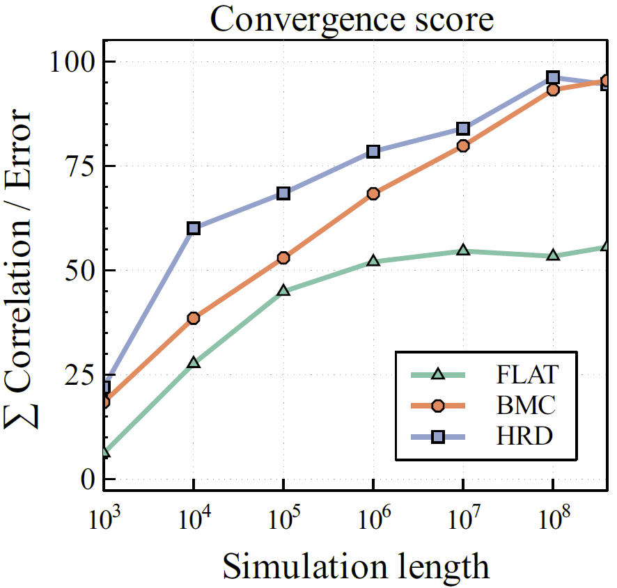 Exploring the design space of the memory hierarchy requires the use of effective methodologies, tools, and models to evaluate different parameter values. Reuse distance is of one of the locality models used in the design exploration and permits analytical cache miss estimation, program characterization, and synthetic trace generation. Unfortunately, the reuse distance is limited to a single locality granularity. Hence, it is not a suitable model for caches with hybrid line sizes, such as sectored caches, an increasingly popular choice for large caches. In this project, we introduce a generalization to the reuse distance, which is able to capture locality seen at multiple granularities. We refer to it as Hierarchical Reuse Distance (HRD). The proposed model has same profiling and synthesis complexity as the traditional reuse distance, and our results show that HRD reduces the average miss rate error on sectored caches by more than three times. In addition, it has superior characteristics in exploring multi-level caches with conventional single line size. For instance, our method increases the accuracy on L2 and L3 by a factor of 4 and converges three orders of magnitude faster.
Modular Reinforcement Learning for Self-Adaptive Multicore
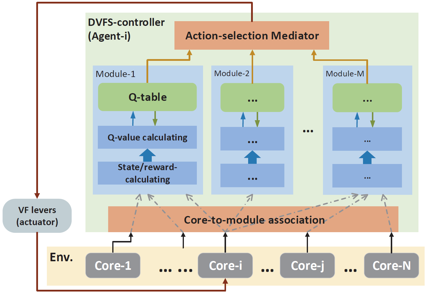 Energy-efficiency is crucial to modern computing systems with multi-/many-core architectures. Dynamic Voltage and Frequency Scaling (DVFS), as an effective low-power technique, has been widely applied to improve energy-efficiency in commercial multi-core systems. However, due to the large number of cores and growing complexity of emerging applications, it is difficult to efficiently find a globally optimized voltage/frequency assignment at runtime. In order to improve the energy-efficiency for the overall multicore system, we propose an online DVFS control strategy based on core-level Modular Reinforcement Learning (MRL) to adaptively select appropriate operating frequencies for each individual core. Instead of focusing solely on the local core conditions, MRL is able to make comprehensive decisions by considering the running-states of multiple cores without incurring exponential memory cost which is necessary in traditional Monolithic Reinforcement Learning (RL). Experimental results on various realistic applications and different system scales show that the proposed approach improves up to 28% energy-efficiency compared to the recent individual-RL approach.
Quantized Power Management for Many-Core Processors
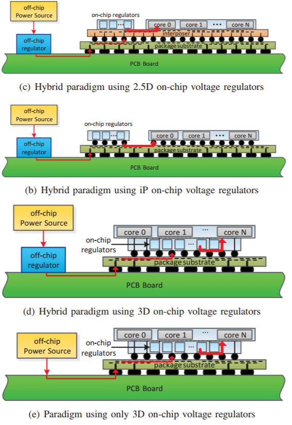 The design of power delivery system plays a crucial role in guaranteeing the proper functionality of many-core processor systems. The power loss on power delivery has become a salient part of total energy consumption, and the energy efficiency of a highly dynamic system has been significantly challenged. Being able to achieve a fast response time and multiple voltage domain control, on-chip voltage regulators(VRs) have become popular choices to enable fine-grain power management, which also enlarge the design space of power delivery systems. This project proposes quantized power management scheme. We compares different power delivery system paradigms and power management schemes in terms of energy efficiency, area overhead and power pin requirment. The analysis shows that compared to the conventional paradigm with offchip voltage regulators, hybrid paradigms with both on-chip and off-chip voltage regulators are able to maintain high efficiency in a larger range of workloads, though they suffer from low efficiency at light workload. Employed with the quantized power management scheme, the hybrid paradigm can improve the system energy efficiency at light workload by a maximum of 136% compared to the traditional load balanced scheme. Besides this, the in-package hybrid paradigm further shows its advantage in reducing the physical overheads. The results reveal that at 120W workload, it occupies only a 10.94% total footprint area or 39.07% power pins of that of the off-chip paradigm. We conclude that the in-package hybrid paradigm achieves the best trade-offs between efficiency, physical overhead and realization of fine-grain power management.
High-Radix Optical Switch for Software-Defined Server
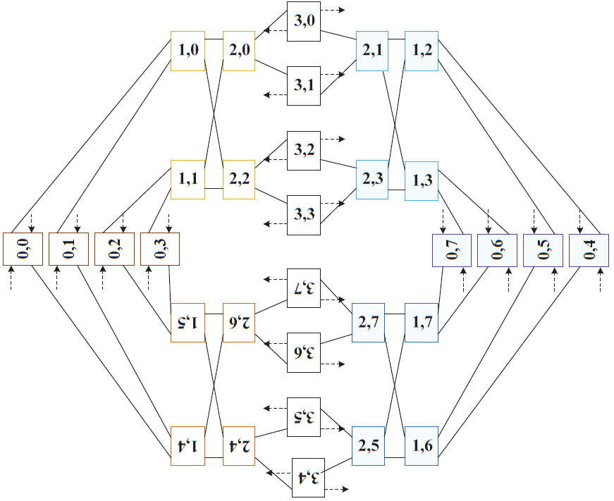 Software-defined servers provide high flexibility and utilization with low energy consumption. To satisfy the ultra-high bandwidth requirement of the interconnection of such servers, integrated optical switch networks, based on the recent development of silicon photonics, are promising candidates. In this project, we proposed a family of Floorplan Optimized Delta Optical Networks (FODON) and novel stage switches. Both the analytical approximation and the loss model based on the exhaustive search approach are developed to evaluate the loss parameters in the networks. The optimization of the stage switch radix is conducted as well. Results show that when 32 WDM channels are employed, the worst-case loss of the 1024 x 1024 FODON with 4 x 4 stage switches is only 26dB, which is 95dB, 63dB, 37dB less than Benes, Fat-tree and Baseline networks of the same size respectively. Furthermore, the average loss and the cost of hardware resources of FODONs are much lower than other networks.
Multiprocessor Simulation Platform Using Statistical Application Models
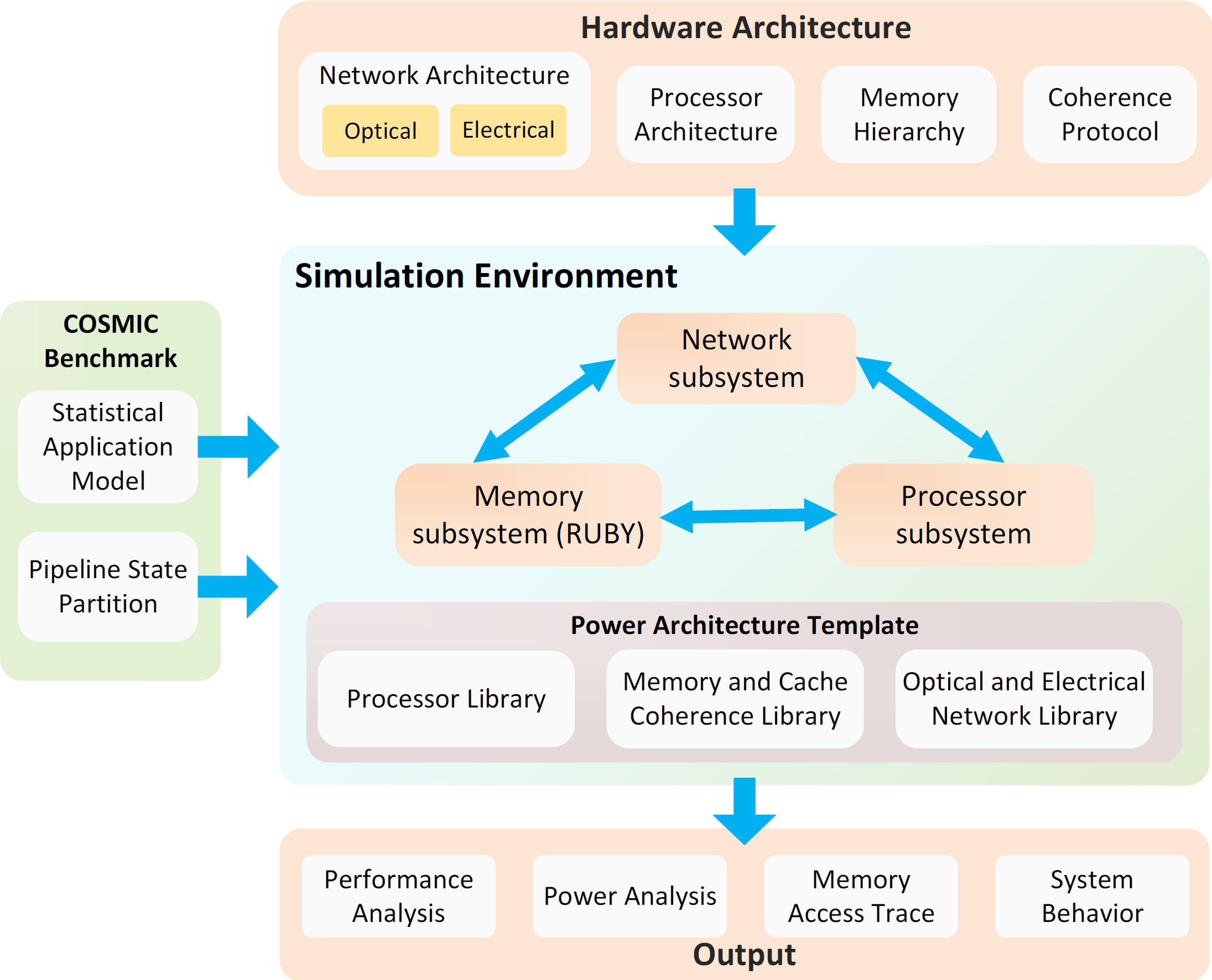 Recent advances in the computing industry towards multiprocessor technologies shifted the dominant method of performance increase from frequency scaling to parallelism. Due to its huge design space, evaluating candidate multicore architectures in early design stages, when the number of variables is at its maximum, is challenging. Simulation plays an important role in estimating architecture performance, and evaluating how the system would perform on average, as well as boundary cases, would require many iterations to cover various cases in the application input domain. Since simulation of heterogeneous systems with enough details are naturally slow, exhaustively evaluating the system for all possible inputs require tremendous amount of time and resources. While there exist quite a few multiprocessor simulators available, they often rely on individual input specification, demanding extensive input enumeration and simulation runs, diminishing their effectiveness for complex systems evaluation. Aiming to fulfill this gap, we publicly release a heterogeneous multiprocessor system simulation platform called JADE, targeting fast initial architecture explorations. Different from most simulators, JADE uses statistical models that follow distributions extracted from internal structures of the application, providing a more convenient and systematic exploration approach to evaluate systems performance. JADE simulation features include detailed electrical and optical interconnections, detailed memory hierarchy infrastructure, and built-in energy analysis allowing studies of a broad spectrum of systems.
On/Off-Chip Power Delivery System Codesign
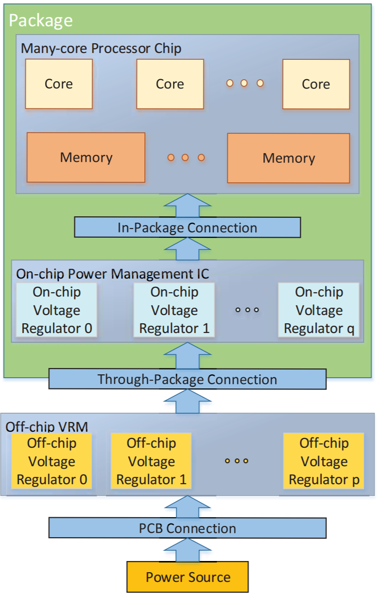 In this project, we propose to codesign on/off-chip power delivery system for multi-core processor for higher energy efficiency and power pin reduction. An analytical model of a power delivery system, consisting of on/off-chip regulators and a power delivery network, is proposed, to evaluate the influence of regulator design and package conduction loss. By combining this model with a multi-core processor model of performance and memory bandwidth requirements, we characterize the entire multi-core processor system to investigate the relationship between the chip pin constraint and performance in multi-core processor scaling, and the effectiveness of our strategy. Experiments show that with the conventional power delivery system design, the chip pin constraint severely limits the performance growth as the technology scales. Using the on/off-chip power delivery system co-design, our strategy achieves a significant pin count reduction, e.g., 31.3% at the 8nm technology node, compared to the conventional design with the same chip performance, while, provided with the same chip pin count, it is able to improve, by 35.0%, the chip performance at 8nm compared to the conventional design. For real applications of different parallelism, our strategy outperforms its counterpart, with a 23.7% performance improvement on average at the 8nm technology node.
I2CON Inter/Intra-Chip Optical Network for Manycore
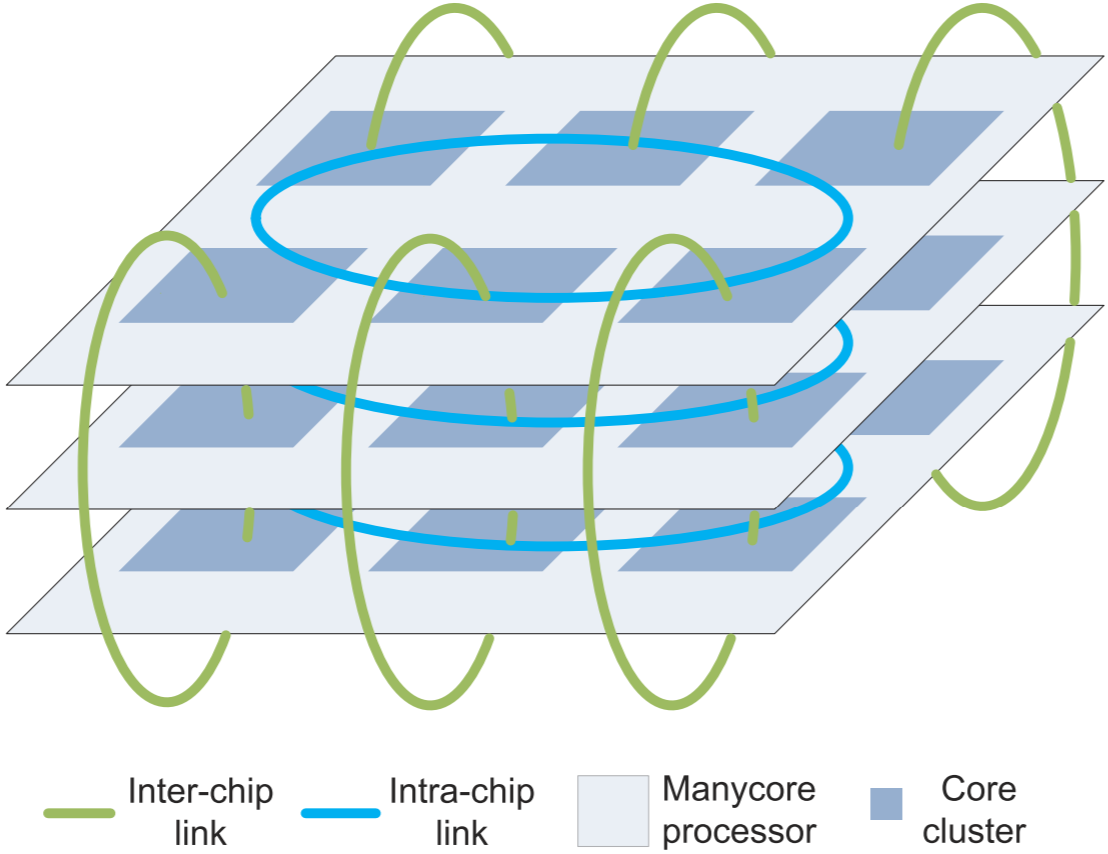 Manycore processor system is becoming an attractive platform for applications seeking both high performance and high energy efficiency. However, huge communication demands among cores, large power density, and low process yield will be three significant limitations for the scalability of future manycore processors. Breaking a large chip into multiple smaller ones can alleviate the problems of power density and yield, but would worsen the problem of communication efficiency due to the limited off-chip bandwidth. In this project, we propose an inter/intra-chip optical network, which will not only fulfill the intra-chip communication requirements but also address the inter-chip communication, by exploiting the advantages of optical links with high bandwidth and energy efficiency. The network is composed of an inter-chip subnetwork and multiple intra-chip subnetworks, and the subnetworks closely coordinate with each other to balance the traffic. The proposed network effectively explores the distinctive properties of optical signals and photonic devices, and dynamically partitions each data channel into multiple sections. Each section can be utilized independently to boost performance as well as reduce energy consumption. Simulation results show that our network can achieve higher throughput with lower power consumption than alternative designs under most of synthetic traffics and real applications.
COSMIC Heterogeneous Multiprocessor Benchmark Suite
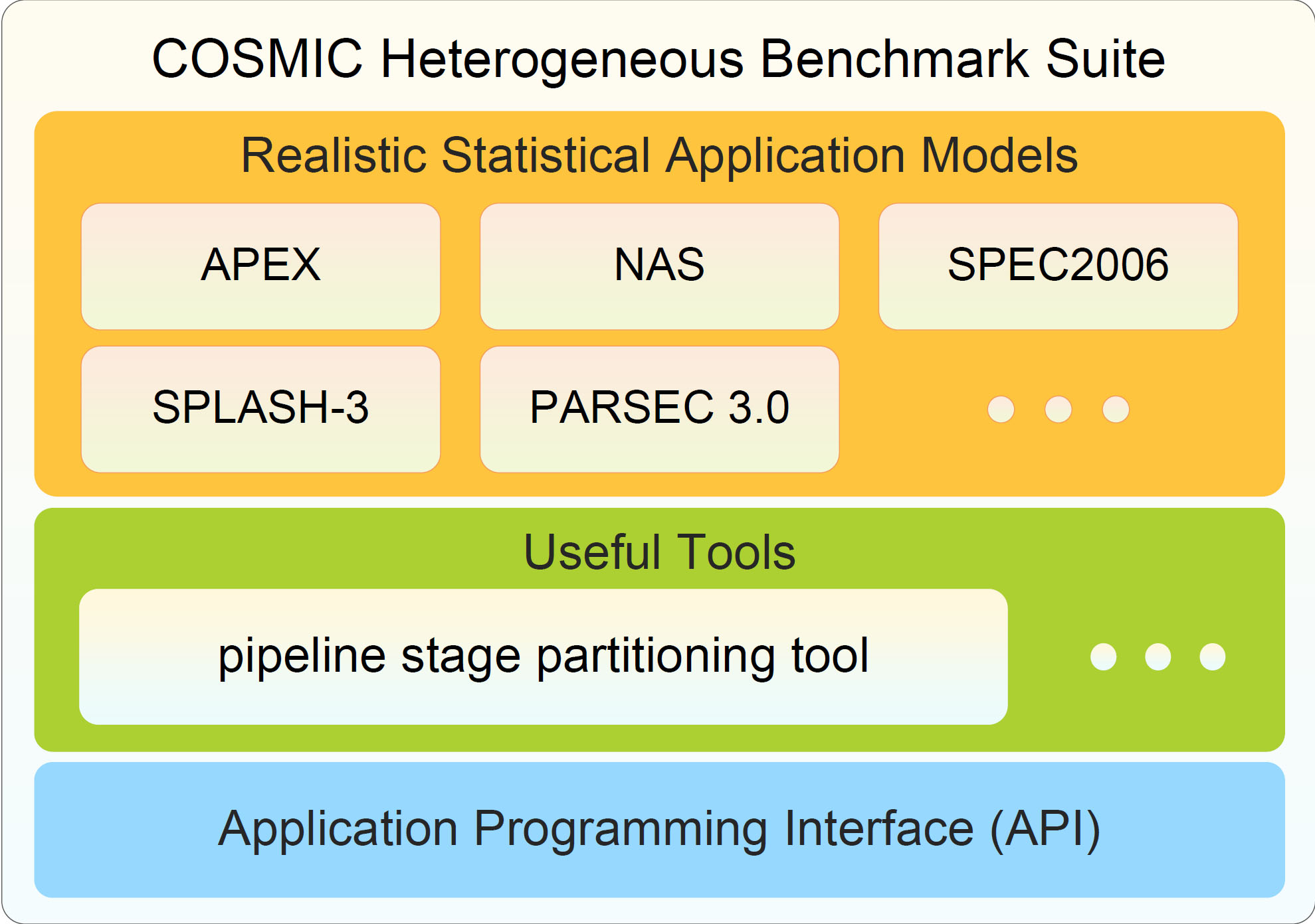 Heterogeneous multiprocessor/multicore/manycore systems are promising alternatives to traditional homogeneous multiprocessor systems and can potentially offer better tradeoffs among energy efficiency, performance, flexibility, scalability, and cost. However exploring their heterogeneities is not well supported by traditional benchmarks which rely on compliers and operating systems developed for homogenous multiprocessor systems. To overcome these issues, this project developed a heterogeneous multiprocessor benchmark suite called COSMIC (Communication-Observant Schedulable Memory-Inclusive Computation). COSMIC is systematically developed from the algorithms of typical multiprocessor applications. Besides implementing the applications in high-level programming languages, COSMIC uses a formal computational model TCG to explicitly capture the computation and communication requirements of multiprocessor applications. It provides a tool to automatically allocate memory and partition and schedule tasks based on user-defined methods.
Optical Thermal Effects in WDM-Based Networks
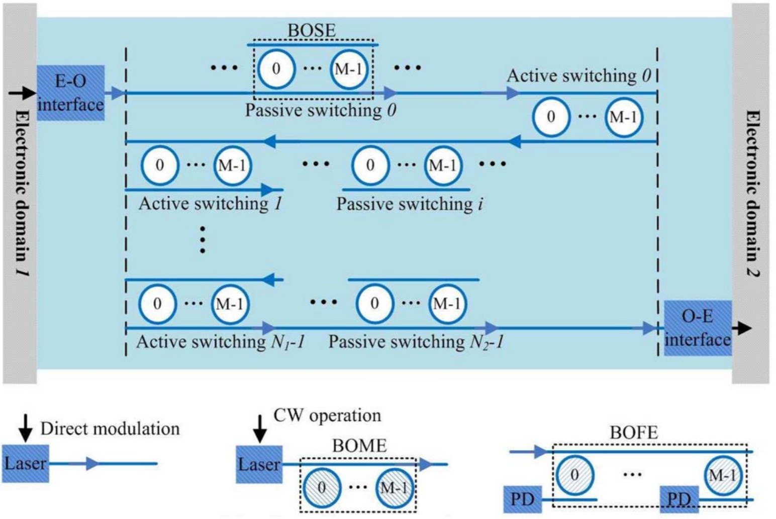 Thermal sensitivity of photonic devices is one of the main concerns about the integrated optical interconnects. We systematically modeled thermal effects in optical links in WDM-based networks. Based on the proposed thermal models, we developed OTemp, an optical thermal effect modeling platform for optical links in both WDMbased ONoCs and single-wavelength ONoCs. OTemp can be used to simulate the power consumption as well as optical power loss for optical links under temperature variations. We use case studies to quantitatively analyze the worst-case power consumption for one wavelength in an eight-wavelength WDM-based optical link under different configurations of low-temperaturedependence techniques. Results show that the worst-case power consumption increases dramatically with on-chip temperature variations. Thermal-based adjustment and optimal device settings can help reduce power consumption under temperature variations. Assume that off-chip vertical-cavity surface-emitting lasers are used as the laser source with WDM channel spacing of 1 nm, if we use thermal-based adjustment with guard rings for channel remapping, the worst-case total power consumption is 6.7 pJ/bit under the maximum temperature variation of 60 C; larger channel spacing would result in a larger worst-case power consumption in this case. If we use thermal-based adjustment without channel remapping, the worst-case total power consumption is around 9.8 pJ/bit under the maximum temperature variation of 60 C; in this case, the worst-case power consumption would benefit from a larger channel spacing.
Manycore Power Delivery System with On-Chip Voltage Regulators
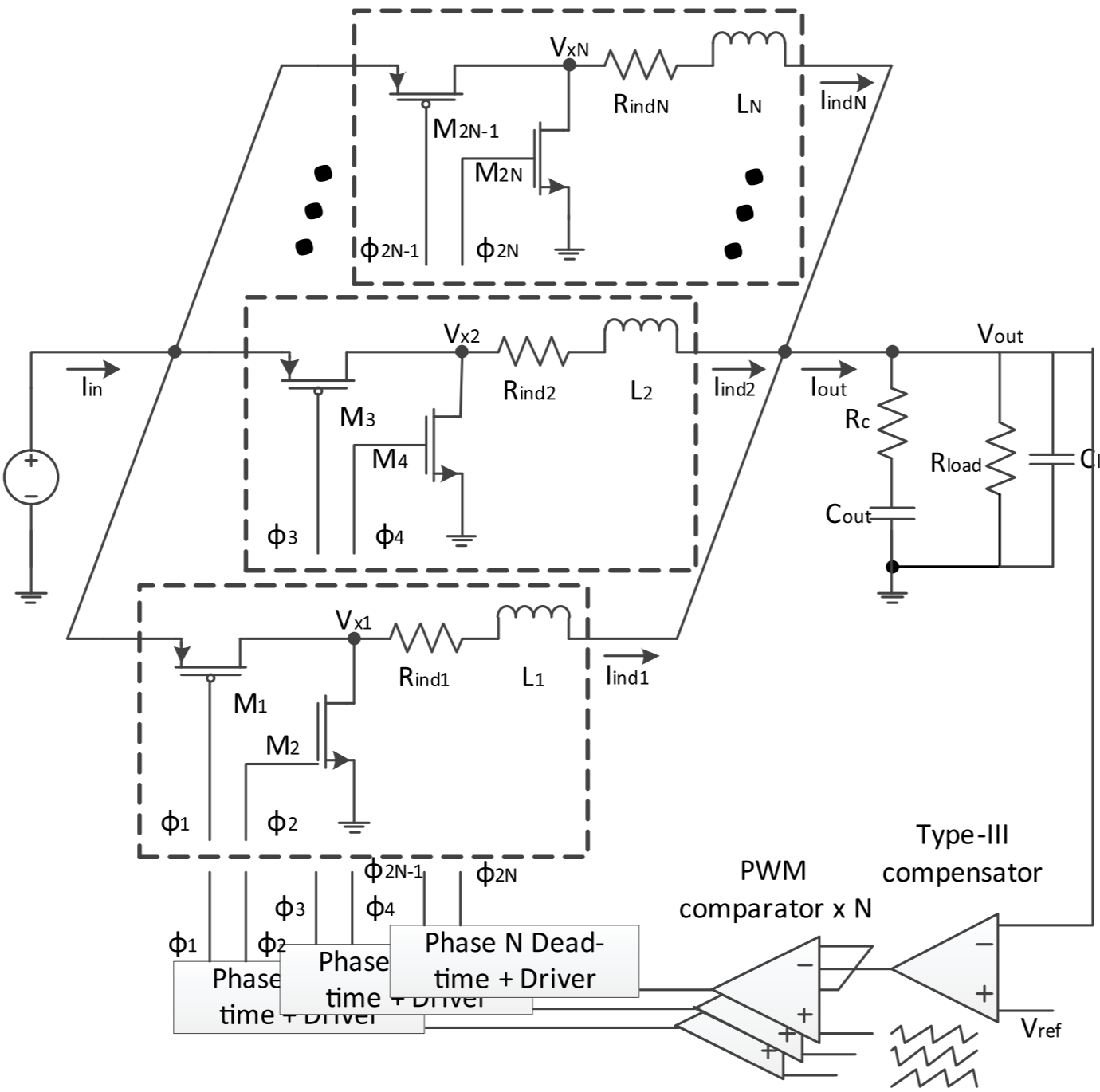 In this project, we present a novel analysis and design optimization platform of power delivery system called power supply on-chip (PowerSoC). It employs an analytical model to provide an accurate and fast evaluation of important characteristics, e.g., power efficiency, output stability, and dynamic voltage scaling, for the entire power delivery system consisting of on-chip/off-chip buck converters and power delivery network. Based on our model, geometric programming is utilized to find the optimal design for different power delivery systems and explore the tradeoff of using on-chip converters. Compared with SPICE simulations, our model achieves a simulation time reduction of six to seven orders of magnitude within 5% model error for the characteristic evaluation of different power delivery systems. By using PowerSoC, various architectures of power delivery systems are optimized for power efficiency under constraints of output stability, area, etc. Simulation results show that the hybrid architecture, consisting of both on-chip and off-chip converters, achieves 1.0% power efficiency improvement and 66.4% area reduction of converters, compared to the conventional design. We conclude the hybrid architecture has potential for efficient dynamic voltage scaling, small area, and the adaptability of the change of power delivery network parasitic, but careful account for the overhead of on-chip converters is needed.
Holistic Modelling and Analysis of Optical-Electrical Interfaces
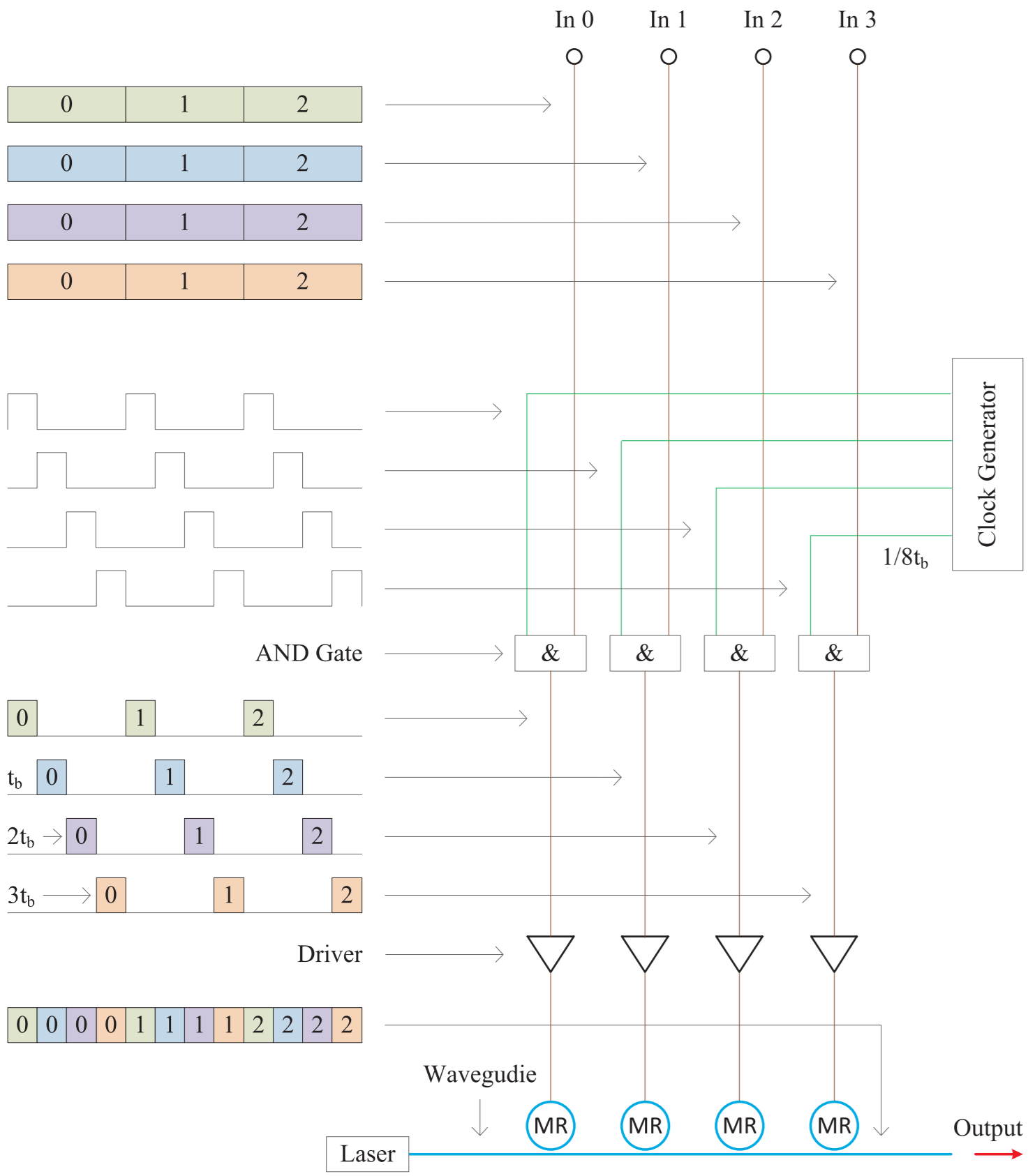 Electrical–optical (E-O) interfaces and optical–electrical (O-E) interfaces are a pair of components that convert data between parallel electrical interconnects and serial optical interconnects. This project holistically models and analyzes E-O and O-E interfaces in terms of energy consumption, area, and latency. Traditional interfaces, where data are converted between parallel and serial ports by serializers and deserializers (SerDes), are studied. A new type of E-O and O-E interface, which serializes and deserializes data by optical weaving technologies, are proposed. Traditional interfaces will become a bottleneck for the further development of optical interconnects in the near future because of the high energy consumption and large area of SerDes necessitating new technologies. Our analysis shows that optical weaving interfaces have a better overall performance than traditional interfaces. For example, if there are 64 parallel electrical interconnects and four optical wavelengths, optical weaving interfaces can achieve a 81.6% improvement in energy consumption and a 40.8% improvement in area, compared with traditional interfaces.
Distributed Sensor Network on Chip
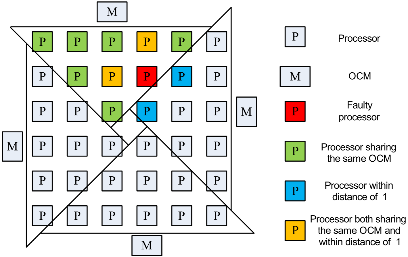 Reliability issues raised by more frequently appeared soft errors are becoming even more critical to the next-generation multiprocessor systems. In this project, we present a systematic approach to address the soft-error problem in multiprocessor system-on-chip with the consideration of system performance optimization. To guarantee the system correctness, distributed senesor network on chip is proposed to protect the processors from soft errors. Tiny hardware sensors are embedded in the processor cores to detect the soft errors, and the software-based rollback scheduling mechanisms are applied for error recovery. The protection costs on hardware duplication and software redundancy are effectively reduced. To optimize the system performance, a distributed control system is built on top of the on-chip communication network and collaboratively manages the entire chip for application execution. With the cluster-based task migration techniques, an efficient runtime task remapping and rescheduling algorithm is proposed to further mitigate the overheads induced by soft-error protection and to minimize the total performance degradation. The distributed control strategy makes the system more adaptable and flexible to the development of the next-generation hardware and software with larger scales. Extensive performance evaluations using SystemC-based cycleaccurate simulations on a set of real-world applications show that our approach has on average 49% performance improvement and 79.6% energy consumption reduction compared with the related state-of-the-art techniques, and hardware synthesis results show that our approach only introduces 2.9% chip area overheads.
Improve Chip Pin Performance Using Optical Interconnects
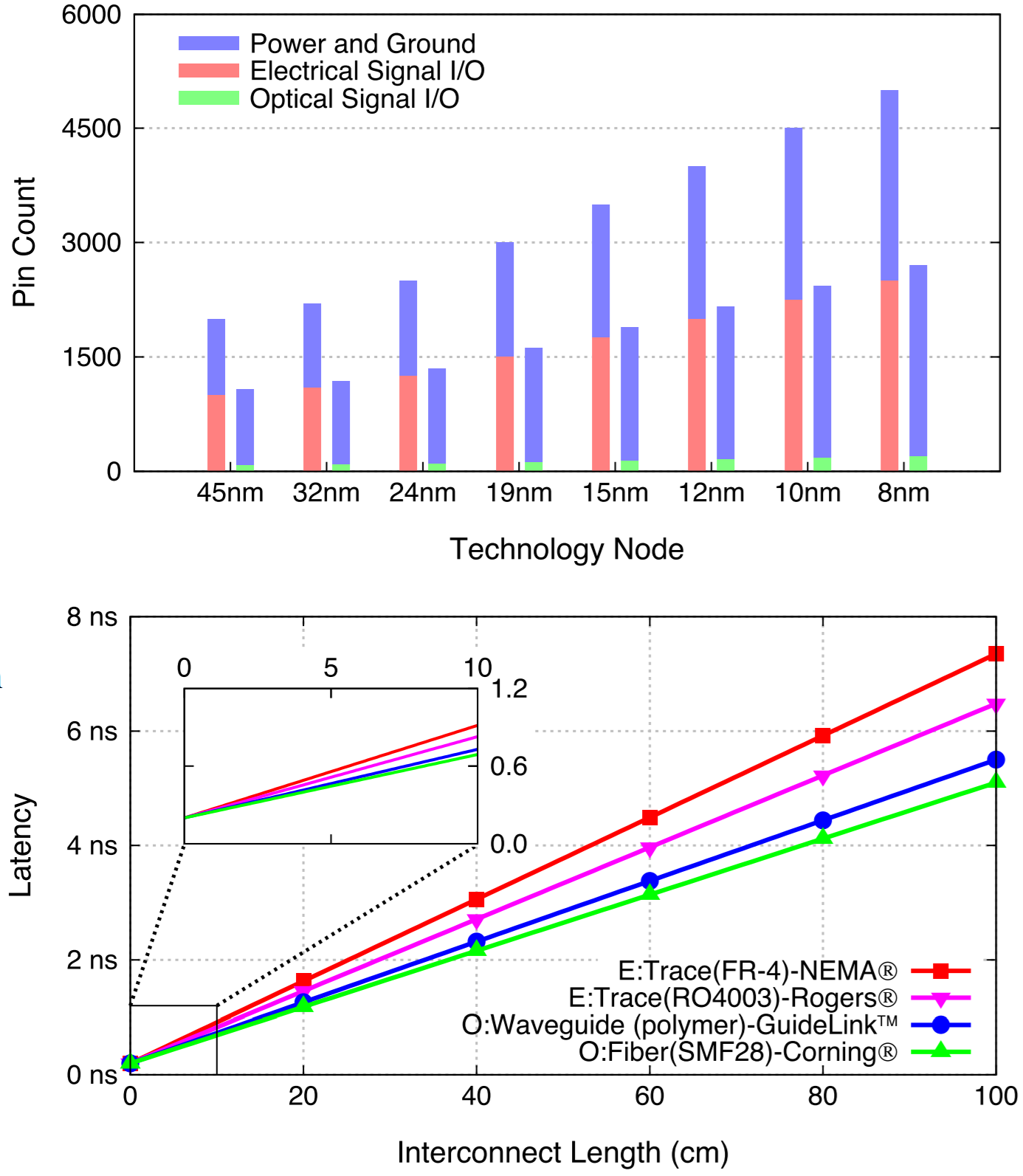 With the fast development of processor chips, power-efficient, high-bandwidth, and low-latency interchip interconnects become more and more important. Studies show that the bandwidth of traditional parallel interconnects with low I/O clock frequencies will become bottlenecks in the near future. To solve this problem, two types of high-bandwidth interchip interconnects are developed. Low-swing differential electrical interconnects have widely been used in high-speed I/O designs. On the other hand, optical interconnects promise high bandwidth, low latency, and could improve the chip pin performance for manycore processors. They are becoming potential alternatives for electrical interconnects. This project systematically models these two types of interconnects in terms of crosstalk noises, attenuation, and receiver sensitivities. Based on the proposed models, we developed optical and electrical interfaces and links (OEIL) and an analysis tool for OEIL. The OEIL can be used to analyze the energy consumption, bandwidth density, and latency of interconnects. Analytical models are verified by the results of published experiments. It shows that the optical interconnects have much higher bandwidth densities than the electrical interconnects. With this feature, the optical interconnects can significantly reduce I/O pin count compared with the electrical interconnects. For example, they can save at least 92% signal pins when connecting chips more than 25 cm (10 in) apart. The energy consumption of optical interconnects is comparable with that of electrical interconnects, and the latency of polymer waveguidebased optical interconnects is 18% less than that of electrical interconnect.
Coherent and Incoherent Crosstalk Noise in Inter/Intra-Chip Optical Networks
 In this project, we develop the analytical models considering both coherent and incoherent crosstalk for both the interchip and intrachip optical networks. The interchip/intrachip optical interconnection networks—the I2CON—are analyzed as a case study. The quantitative results on the individual networks have demonstrated that the architectural design determines the impact of crosstalk on the SNR. We have also demonstrated that the optical interconnection networks with interchip/intrachip interconnects result in better bit error rate (BER) compared with that of only intrachip interconnect. Our analyses of the worst case can be utilized as a platform to compare the realistic performance among different optical interconnection networks via the degradation of SNR/BER and data bandwidth.
Optimal Fat-Tree-based Multiprocessor Floorplan
 Chip multiprocessor (CMP) is becoming increasingly popular. Fat-tree based on-chip network has many advantages over traditional mesh or torus based networks in terms of throughput, power efficiency and latency. However, the floorplan of the fat-tree based NoC is very challenging because of the complexity of topology. There are a large number of crossings and long interconnects, which cause severe performance degradation in the network. In electronic NoCs, the parasitic capacitance and inductance will be significant. In optical ones, large crosstalk noise and power loss will be introduced. The novel contribution of this project is to propose a method to optimize the fat-tree floorplan, which can effectively reduce the number of crossings and minimize the interconnect length. Two types of floorplans are proposed, which could be applied to fat-tree based networks of arbitrary size. Compared with the traditional one, our floorplans could reduce more than 87% of the crossings. Since the traversal distance for signals is related to the aspect ratio of the processor cores, we also present a method to calculate the optimum aspect ratio of the processor cores to minimize the traversal distance.
SUOR: Sectioned Undirectional Optical Ring for Multiprocessor
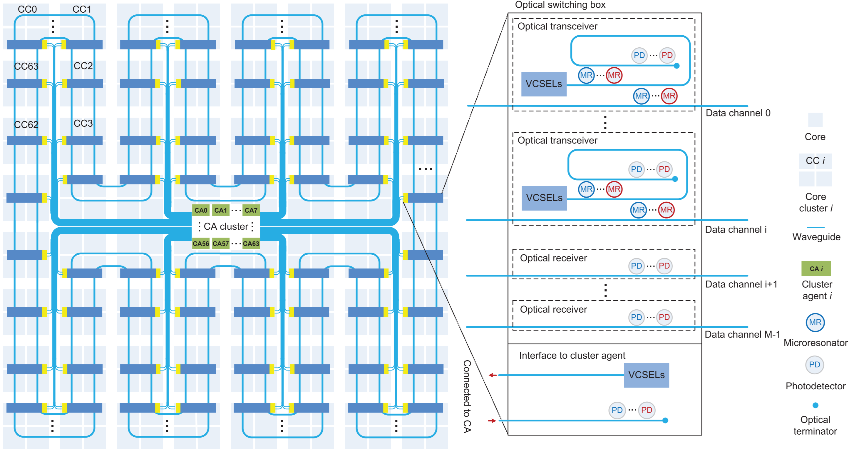 Chip multiprocessor (CMP) is becoming an attractive platform for applications seeking both high performance and high energy efficiency. In large-scale CMPs, the communication efficiency among cores is crucial for the overall system performance and energy consumption. In this project, we propose a ring-based optical network-on-chip, called SUOR, to fulfill the communication requirement of CMPs. SUOR effectively explores the distinctive properties of optical signals and photonic devices, and dynamically partitions each data channel into multiple sections. Each section can be utilized independently to boost performance as well as reduce energy consumption. We develop a set of distributed control protocols and algorithms for SUOR, but physically allocate the corresponding cluster agents close to each other to benefit from the strengths of optical interconnects at long distances as well as electrical interconnects at short distances. Simulation results show that SUOR outperforms the alternative optical networks under a wide range of traffic patterns. For example, compared with MWSR design, SUOR achieves 2.58X throughput as well as saves 64% energy consumption on average in a 256-core CMP. Compared with MWMR design, SUOR achieves 1.52X throughput and reduces 73% energy consumption on average.
Realistic Traffic Patterns for NoC-based MPSoC
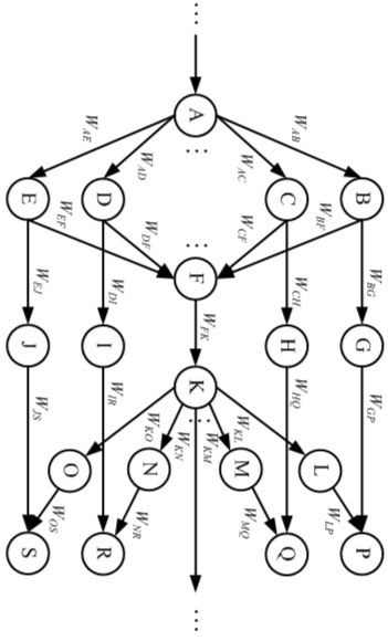 As programs for microprocessor architectures, network-on-chip (NoC) traffic patterns are essential tools for NoC-based MPSoC performance assessments and architecture explorations. The fidelity of NoC traffic patterns has profound influence on NoC studies. For the first time, this project presents a set of realistic traffic patterns, called MCSL, and the methodology used to generate it. The publicly released MCSL NoC traffic patterns includes eight real applications and covers popular NoC architectures. It captures not only the communication behaviors in NoCs but also the temporal dependencies among them. MCSL traffic patterns can be easily incorporated into existing NoC simulators and significantly improve NoC simulation accuracy. We developed a systematic traffic generation methodology to create MCSL based on real applications. The methodology uses formal computational models to capture both communication and computation requirements of applications. It optimizes application mapping and scheduling to faithfully maximize overall system performance and utilization before extracting realistic traffic patterns through cycle-accurate simulations. Experiment results show that MCSL traffic patterns can be used to study NoC characteristics more accurately than traditional random traffic patterns.
Process-Variation-Aware Mitigation of MPSoC Power/Ground Noise
 Power gating (PG) is the most effective techniques to reduce the leakage power in multiprocessor system-on-chips (MPSoCs). However, the power-mode transition during the PG period of an individual processing unit (PU) will introduce serious power/ground (P/G) noise to the neighboring PUs. As technology scales, the P/G noise problem becomes a severe reliability threat to MPSoCs. At the same time, the increasing manufacturing process variations (PVs) also bring uncertainties to the P/G noise problem and make it difficult to predict and mitigate. To tackle this problem, in this project, we analyze the PG-induced P/G noise in the presence of PVs and propose a hardware–software collaborated runtime technique to adaptively protect PUs from P/G noise. Sensor network-on-chip is used to gather noise information and coordinate different system components. An online PV-aware algorithm is developed to effectively decide the noise impact range and arrange protections for affected PUs based on the collected noise information. We evaluate the proposed technique through cycle-level Monte Carlo simulations of NoC-based MPSoCs in different scales. The experimental results on various realistic applications show that our technique could achieve comparable reliability to the most reliable static technique while improve on average 3.78%–29.5% the system energy efficiency and reduce 15.7%–70.4% the performance penalty on different MPSoC scales.
UNION: Unified Inter/Intra-Chip Optical Network
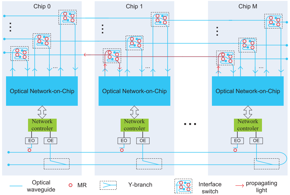 As modern computing systems become increasingly complex, communication efficiency among and inside chips has become as important as the computation speeds of individual processing cores. Traditionally, to maximize design flexibility, interchip and intrachip communication architectures are separately designed under different constraints. Jointly designing communication architectures for both interchip and intrachip communication could, however, potentially yield better solutions. In this project, we present a unified inter/intrachip optical network, called UNION, for chip multiprocessors (CMPs). UNION is based on recent progresses in nanophotonic technologies. It connects not only cores on a single CMP, but also multiple CMPs in a system. UNION employs a hierarchical optical network to separate interchip communication traffic from intrachip communication traffic. It fully utilizes a single optical network to transmit both payload and control packets. The network controller on each CMP not only manages intrachip communications, but also collaborates with each other to facilitate interchip communications. We compared UNION with a matched electrical counterpart in 45-nm process. Simulation results for eight real CMP applications show that on average UNION improves CMP performance by 3× while reducing 88% of network energy consumption.
Alleviate Power/Ground Noise Using On-Chip Memories
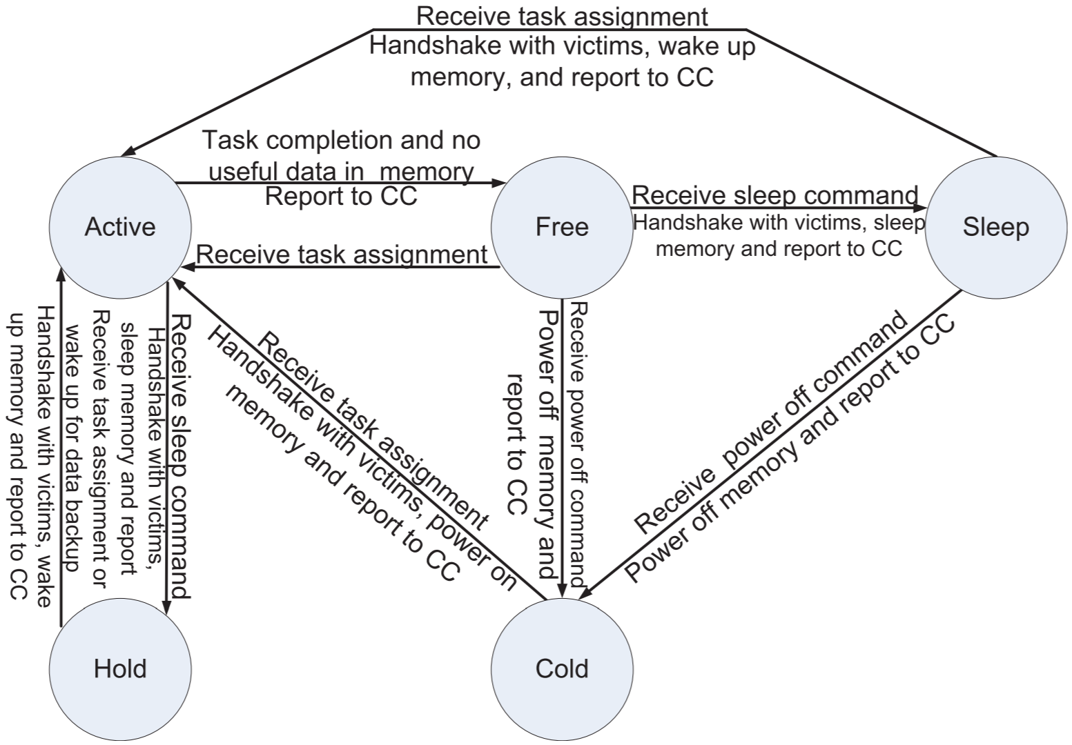 By integrating multiple processing units (PUs) and memories on a single chip, multiprocessor system-on-chip (MPSoC) can provide higher performance per energy and lower cost per function to applications with growing complexity. On the other hand, shrinking feature sizes and reducing power supply voltages also make MPSoCs more susceptible to various reliability threats, such as power/ground (P/G) noises. Power gating is an effective technique to minimize leakage power. However, it also introduces significant P/G noises in MPSoCs. With significant area, power and performance overheads, traditional methods rely on reinforced circuits or fixed protection strategies to reduce P/G noises caused by power gating. In this project, we propose a systematic approach to actively alleviating P/G noises using the parasitic capacitance of on-chip memories through sensor network on-chip (SENoC). We use the parasitic capacitance of on-chip memories as dynamic decoupling capacitance to suppress P/G noises and develop a detailed HSPICE model for related study. SENoC is developed to not only monitor and report P/G noises, but also coordinate PUs and memories to alleviate such transient threats at run time. Extensive evaluations show that compared with traditional method, our approach saves 12.6%–62.8% energy consumption and achieves 14.3%–69.8% performance improvement for different applications and MPSoCs with different scales. We implement the circuit details of our approach and show its low area and energy consumption overheads.
SNR of Ring-Based Optical Networks
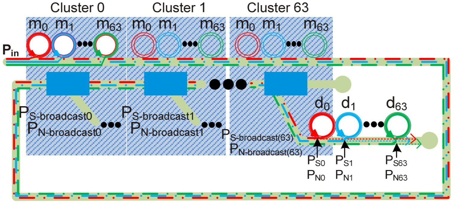 Microresonators have been utilized to construct optical interconnection networks. One of the drawbacks of these microresonators is that they suffer from intrinsic crosstalk noise and power loss, resulting in Signal-to-Noise Ratio (SNR) reduction and system performance degradation at the network level. The novel contribution of this project is to systematically study the worst-case crosstalk noise and SNR in a ring-based ONoC, the Corona. In the paper, Corona’s data channel and broadcast bus are investigated, with formal general analytical models presented at the device and network levels. Leveraging our detailed analytical models, we present quantitative simulations of the worst-case power loss, crosstalk noise, and SNR in Corona. Moreover, we compare the worst-case results in Corona with those in mesh-based and folded-torus-based ONoCs, all of which consist of the same number of cores as Corona. The quantitative results demonstrate the damaging impact of crosstalk noise and power loss in Corona: the worst-case SNR is roughly 14.0 dB in the network, while the worst-case power loss is substantially high at -69.3 dB in the data channel.
Hardware-Software Collaborated Method for Soft-Error Tolerant MPSoC
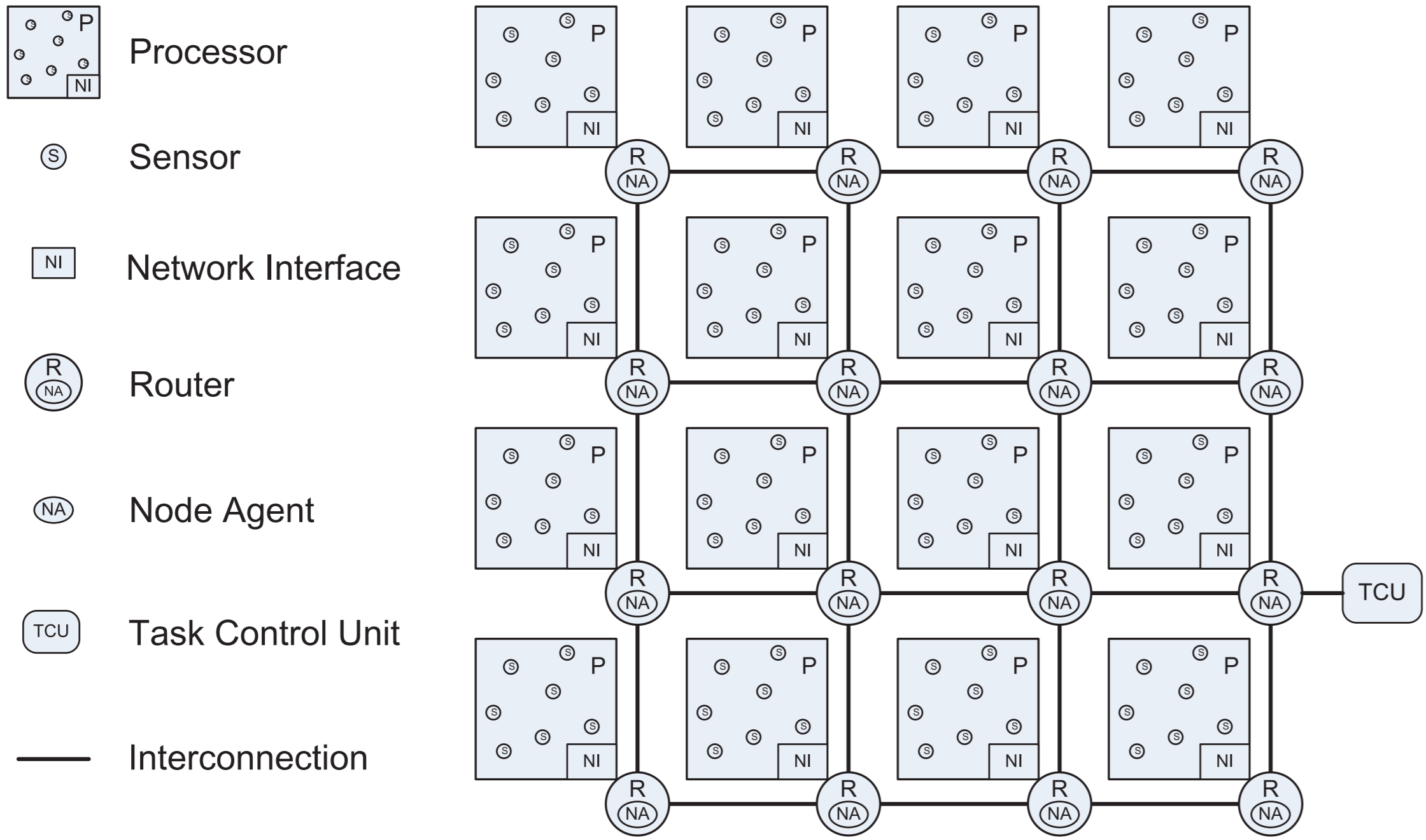 Multiprocessor systems-on-chip (MPSoCs) are attractive platforms for embedded applications with growing complexity, because integrating a system or a complex subsystem on a single chip provides better performance and energy efficiency and lower cost per function. As feature sizes and power supply voltages continually decrease, MPSoCs are becoming more susceptible to soft errors. However, traditional soft-error tolerant methods introduce large area, power and performance overheads to MPSoCs. This project proposes a low-overhead hardware-software collaborated method to dynamically mitigate soft errors on MPSoCs using an on-chip sensor network. We developed a low-cost on-chip sensor network to collaboratively monitor and detect soft errors, and implemented software-based mechanisms to guarantee correct task executions. To maximize the performance of soft-error tolerant MPSoCs, a hybrid scheduling scheme is proposed to effectively manage applications and resources under uncertainties. We studied the new method on MPSoCs with different scales and tested it using typical embedded applications under different cosmic ray flux conditions. Experimental results show that comparing to traditional methods our method requires substantially lower protection overheads to achieve the same level of soft-error tolerance.
Formal Study on Floorplan Characteristics of Optical Networks-on-Chip
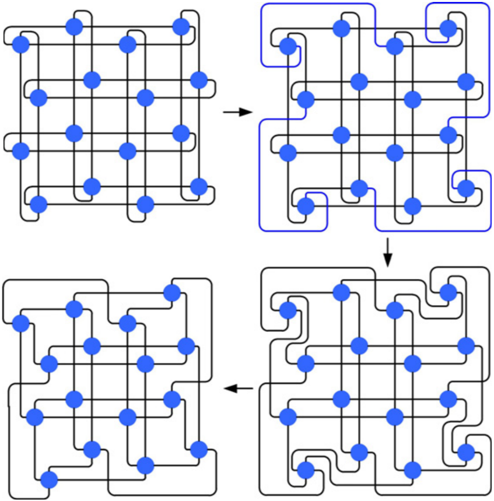 This project provides the first detailed study on the floorplans of optical network-on-chips in three popular topologies: mesh, torus, and fattree. The study covers important design metrics ONoCs, such as the number of waveguide crossings in the floorplan and the number of paths and hops. We summarize the results into equations, taking all the dimensional cases into consideration. We propose several approaches to systamtically optimize the power efficiency of ONoCs by minimizing the number of waveguide crossings in the floorplan. Comparison results show that the floorplan optimization reduces waveguide crossings significantly within the entire network as well as in longest paths.
System-Level Modeling and Analysis of Thermal Effects in Optical Interconnects
 The performance of multiprocessor systems, such as chip multiprocessors (CMPs), is determined not only by individual processor performance, but also by how efficiently the processors collaborate with one another. It is the communication architecture that determines the collaboration efficiency. Optical networks-on-chip (ONoCs) are emerging communication architectures that can potentially offer ultra-high communication bandwidth and low latency to multiprocessor systems. Thermal sensitivity is an intrinsic characteristic of photonic devices used by ONoCs as well as a potential issue. This project systematically modeled and quantitatively analyzed the thermal effects in ONoCs. We revealed three important factors regarding ONoC power efficiency under temperature variations, and proposed several techniques to reduce the temperature sensitivity of ONoCs. These techniques include the optimal initial setting of microresonator resonant wavelength, increasing the 3-dB bandwidth of optical switching elements by parallel coupling multiple microresonators, and the use of passive-routing optical routers to minimize the number of switching stages. The findings in this project will support further developments of this emerging technology.
HOME: Hierarchical Hybrid Optical-Electronic NoC
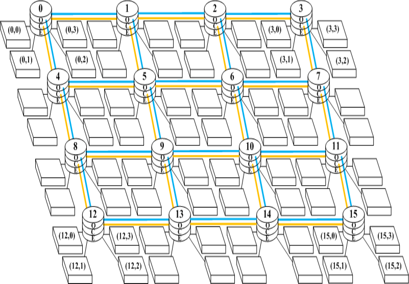 We proposed a hybrid optical mesh NoC, HOME, which utilizes optical waveguides as well as metallic interconnects in a hierarchical manner. HOME employs a new set of protocols to improve the network throughput and latency. We compared HOME with a matched optical mesh NoC for a 64-core MPSoC in 45nm, using SPICE simulations and our cycle-accurate multi-objective NoC simulation platform, MoLab. Comparing with the optical mesh NoC, HOME uses 75% less optical/electronic interfaces and laser diodes. Simulation results show that HOME achieves 17% higher throughput and 40% less latency while consuming 42% less power.
Optical Crosstalk Noise in WDM-based Networks
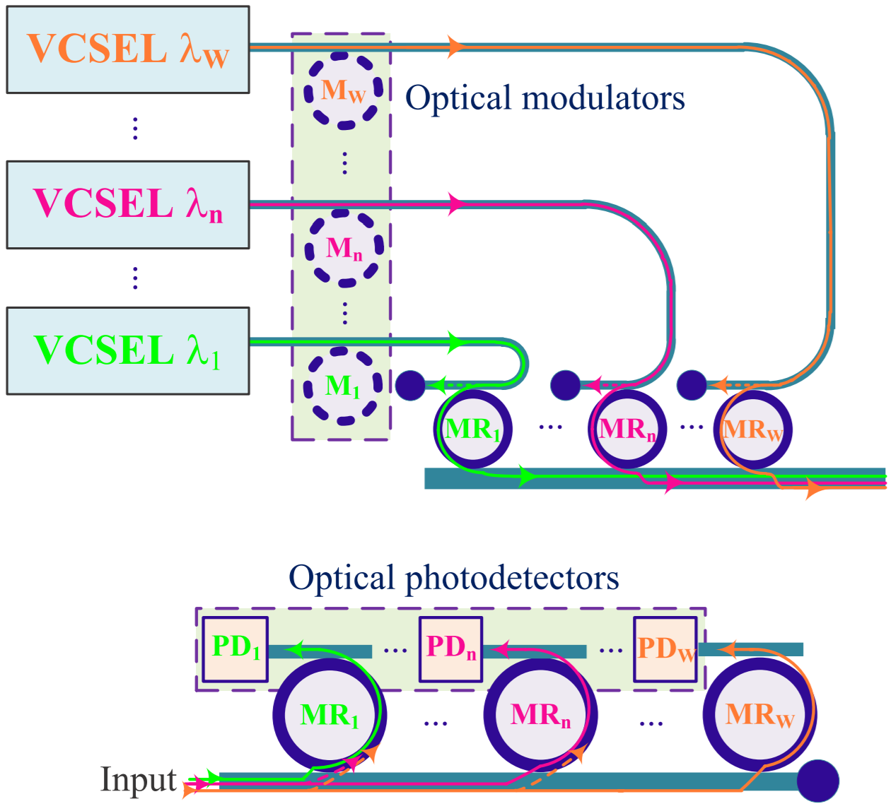 Optical networks using wavelength-division multiplexing (WDM) technology have progressively attracted more and more attention for their use in tackling the high-power consumption and low bandwidth issues in growing metallic interconnection networks in multiprocessor systems-on-chip. However, the basic optical devices employed to construct WDM-based ONoCs are imperfect and suffer from inevitable power loss and crosstalk noise. Furthermore, when employing WDM, optical signals of various wavelengths can interfere with each other through different optical switching elements within the network, creating crosstalk noise. As a result, the crosstalk noise in large-scale WDM-based ONoCs accumulates and causes severe performance degradation, restricts the network scalability, and considerably attenuates the signal-to-noise ratio (SNR). In this project, we systematically study and compare the worst case as well as the average crosstalk noise and SNR in three well-known optical interconnect architectures, mesh-based, folded-torus-based, and fat-tree-based ONoCs using WDM. The analytical models for the worst case and the average crosstalk noise and SNR in the different architectures are presented. Furthermore, the proposed analytical models are integrated into a newly developed crosstalk noise and loss analysis platform (CLAP) to analyze the crosstalk noise and SNR in WDM-based ONoCs of any network size using an arbitrary optical router. Utilizing CLAP, we compare the worst case as well as the average crosstalk noise and SNR in different WDM-based ONoC architectures. Furthermore, we indicate how the SNR changes in respect to variations in the number of optical wavelengths in use, the free-spectral range, and the microresonators Q factor. The analyses’ results demonstrate that the crosstalk noise is of critical concern to WDM-based ONoCs: in the worst case, the crosstalk noise power exceeds the signal power in all three WDM-based ONoC architectures, even when the number of processor cores is small, e.g., 64.
Power Gating Aware MPSoC Task Scheduling
 Shrinking the feature size allows more and better functions on a single chip. However, it makes multiprocessor system-on-chip (MPSoC) more susceptible to various reliability threats. Power supply noise is a major reliability problem faced by low power MPSoCs using power gating techniques. Powering on and off a processing unit in MPSoCs will induce large power/ground (P/G) noise and can cause timing divergence and even functional errors in surrounding processing units. Previous work on resilient architectures mainly focused on power/thermal management and neglected the important side-effect: P/G noise induced by power gating. In this project, for the first time, we formulate a task scheduling problem with the consideration of P/G noise based on our detailed P/G noise analysis platform for MPSoC. Two efficient algorithms are proposed to reduce noise protection penalty and improve MPSoC performance. Our experiments show that both simulated annealing and heuristic algorithms can achieve on average 25% performance improvement together with up to 80% noise protection penalty saving compared with the conservative stop-go method for short tasks (shorter than 20K clock cycles). For longer tasks up to 200K clock cycles, the performance improvement of our methods will become relatively low. However, we can still achieve at least 35.2% noise protection penalty saving. Furthermore, a lightweight online adjustment strategy accompanying the offline scheduling method is proposed to adapt to runtime variations and improve reliability.
Crosstalk Noise and Bit Error Rate of Optical Networks
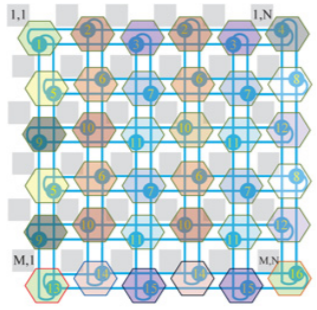 Photonic devices are widely used in optical networks and suffer from crosstalk noise. The accumulative crosstalk noise in large scale optical networks diminishes the signal-to-noise ratio (SNR), causes severe performance degradation, and constrains the network scalability. For the first time, this project systematically analyzes and models the worst-case crosstalk noise and SNR in torus-based ONoCs. Formal analytical models for the worst-case crosstalk noise and SNR are presented. The crosstalk noise analysis is hierarchically performed at the basic photonic device level, then at the optical router level, and finally at the network level. We consider a general 5×5 optical router model to enable crosstalk noise and SNR analyses in folded-torus-based ONoCs using an arbitrary 5×5 optical router. Using the general optical router model, the worst-case SNR link candidates, which restrict the network scalability, are found. Also, we present a novel crosstalk noise and loss analysis platform, called CLAP, which can analyze the crosstalk noise and SNR of arbitrary ONoCs. Case studies of optimized crossbar and Crux optical routers using recent photonic device parameters are presented. Moreover, we compare the worst-case crosstalk noise and SNR in folded-torus-based and mesh-based ONoCs using optimized crossbar and Crux optical routers. The quantitative simulation results show the critical behavior of crosstalk noise in large scale ONoCs. For example, in folded-torus-based ONoCs using the Crux optical router, the noise power exceeds the signal power for network sizes larger than 12×12; when the network size is 20×20 and the injection signal power equals 0 dBm, the signal power and noise power are -9.4 dBm and -6.1 dBm, respectively.
FONoC: Fat Tree-based Optical Networks-on-Chip
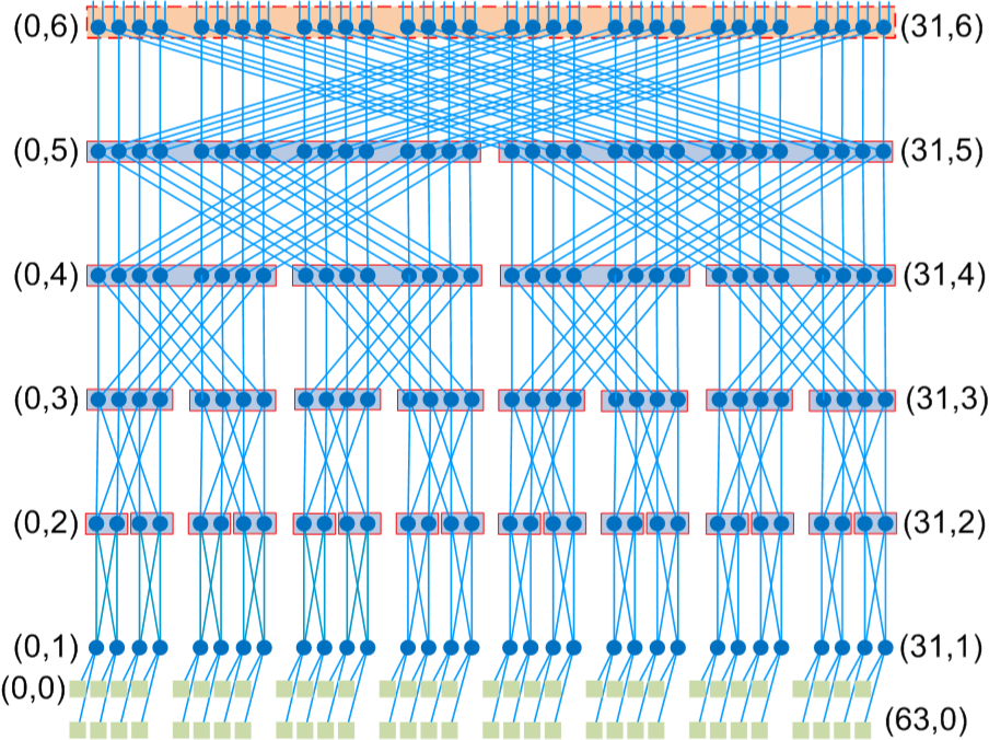 We proposed a fat tree-based optical NoC (FONoC) including its topology, floorplan, protocols, and a low-power and low-cost optical router, optical turnaround router (OTAR). Different from other optical NoCs, FONoC does not require building a separate electronic NoC for network control. It carries both payload data and network control data on the same optical network, while using circuit switching for the former and packet switching for the latter. The FONoC protocols are designed to minimize network control data and the related power consumption. An optimized turnaround routing algorithm is designed to utilize the low-power feature of OTAR, which can passively route packets without powering on any microresonator in 40% of all cases. Comparing with other optical routers, OTAR has the lowest optical power loss and uses the lowest number of microresonators. An analytical model is developed to characterize the power consumption of FONoC. We compare the power consumption of FONoC with a matched electronic NoC in 45 nm, and show that FONoC can save 87% power comparing with the electronic NoC on a 64-core MPSoC. We simulate the FONoC for the 64-core MPSoC and show the end-to-end delay and network throughput under different offered loads and packet sizes.
SENoC: On-Chip Sensor Network
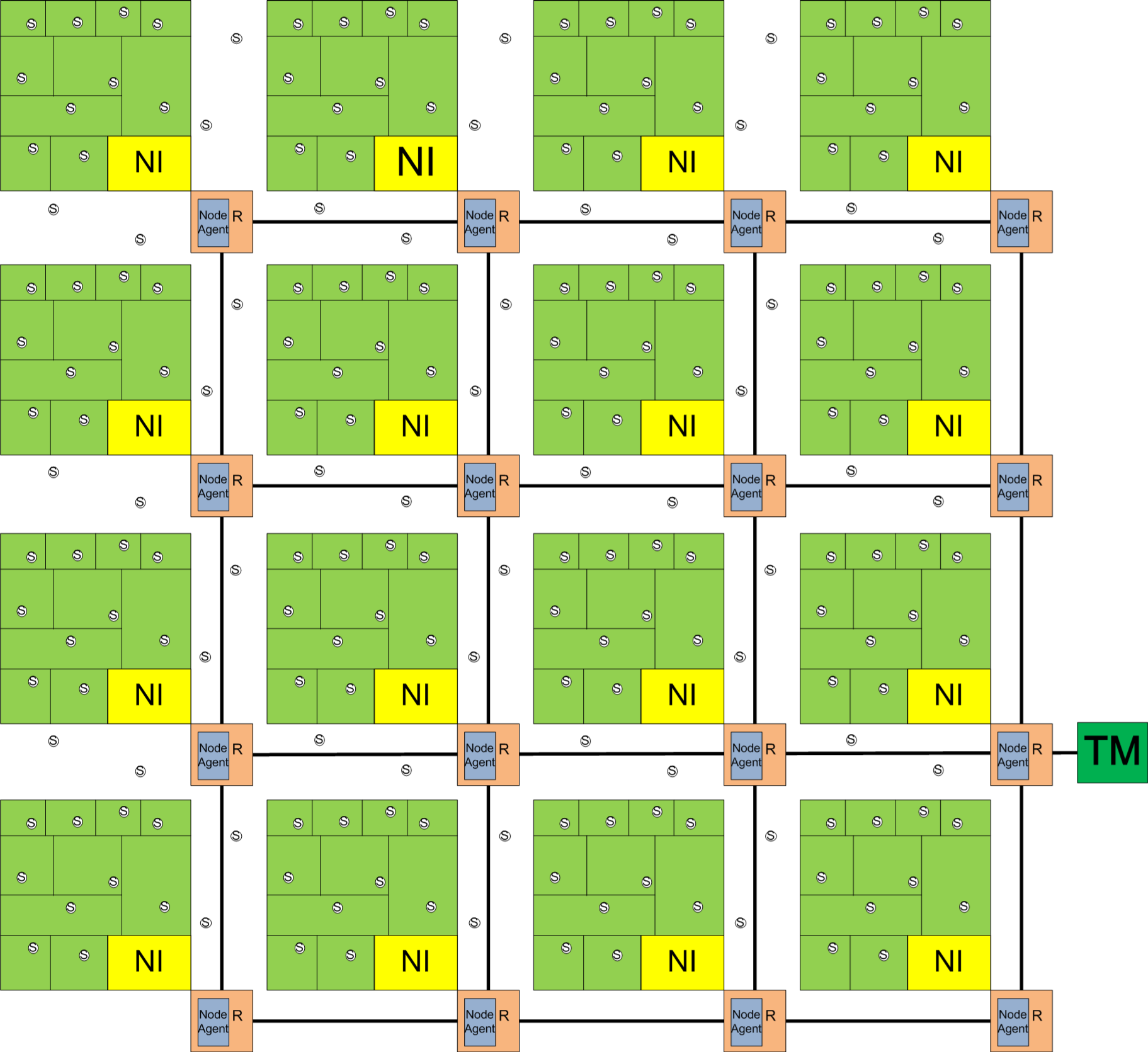 Reducing feature sizes and power supply voltage allows integrating more processing units (PUs) on multiprocessor system on chip (MPSoC) to satisfy the increasing demands of applications. However, it also makes MPSoC more susceptible to various reliability threats, such as high temperature and power/ground (P/G) noise. As the scale and complexity of MPSoC continuously increase, monitoring and mitigating reliability threats at runtime could offer better performance, scalability, and flexibility for MPSoC designs. In this project, we propose a systematic approach, on-chip sensor network (SENoC), to collaboratively predict, detect, report, and alleviate runtime threats in MPSoC. SENoC not only detects reliability threats and shares related information among PUs, but also plans and coordinates the reactions of related PUs in MPSoC. SENoC is used to alleviate the impacts of simultaneous switching noise in MPSoC’s P/G network during power gating. Based on the detailed noise behaviors under different scenarios derived by our circuitlevel MPSoC P/G noise simulation and analysis platform, simulation results show that SENoC helps to achieve on average 26.2 percent performance improvement compared with the traditional stop-go method with 1.4 percent area overhead in an 8*8-core MPSoC in 45 nm. An architecture-level cycle-accurate simulator based on SystemC is implemented to study the performance of the proposed SENoC. By applying sophisticated scheduling techniques to optimize the total system performance, a higher performance improvement of 43.5 percent is achieved for a set of real-life applications.
3D Optical Network-on-Chip for Multiprocessor System-on-Chip
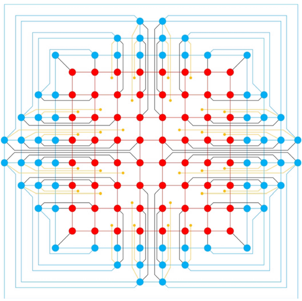 Optical networks-on-chip (ONoCs) are emerging communication architectures that can potentially offer ultra-high communication bandwidth and low latency to multiprocessor systems-on-chip (MPSoCs). Three-dimensional integrated technologies offer an opportunity to continue performance improvements with higher integration densities. In this project, we present a 3D mesh-based ONoC for MPSoCs, and new low-cost non-blocking 4x4, 5x5, 6x6 and 7x7 optical routers for dimension-order routing. Besides, we propose an optimized floorplan for the 3D mesh-based ONoC. The floorplan follows the regular 3D mesh topology but implements all optical routers in a single optical layer. The floorplan is optimized to minimize the number of extra waveguide crossings caused when merging the 3D ONoC to one optical layer.
Resilient Multiprocessor System-on-Chip
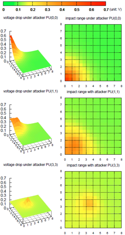 The continuous development of semiconductor technologies makes multiprocessor system-on-chip (MPSoC) an attractive platform to implement high-performance and low-power applications such as network packet processing, wireless baseband, and video processing. The programmability of MPSoC not only reduces development times of complex applications but also spreads non-recurring engineering (NRE) cost over multiple systems and multiple generations of the same system. Furthermore, MPSoC shortens time-to-market by starting system development before an application standard is finalized, and allows continuous enhancement of a system after an initial release. Reliability is a critical issue for MPSoC. MPSoC is required to perform and maintain its functionality under normal circumstances as well as hostile or unexpected circumstances for a specific period of time. On one hand, shrinking feature sizes allows for more and better functions on an MPSoC. On the other hand, an MPSoC with smaller feature sizes is more susceptible to various reliability issues, such as negative bias temperature instability (NBTI) induced aging, soft error, and power grid noise. We proposed a resilient multiprocessor system-on-chip to combat reliability threats.
Application-Specific Networks-on-Chip
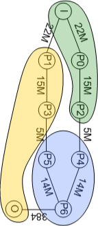 We proposed a novel on-chip communication architecture, the Application-Specific Network-on-Chip (ASNoC). ASNoCs achieve higher performance and lower cost than regular-topology Networks-on-Chip (NoCs) by using network hierarchies, irregular topologies, floorplan estimation, and optimized protocols. We also proposed a systematic ASNoC design methodologies, compatible with current HW/SW codesign flows. Using the methodology, we designed ASNoCs for two SoCs. Results show that the ASNoCs offer significantly higher performance and lower cost than mesh-based networks-on-chip. In a H.264 HDTV decoder SoC, the ASNoC consumes only 61% power, 41% silicon area, 26% metal area, 37% switch capacity, and 31% interconnection capacity to achieve 201% performance compared with a regular-topology NoC.
Cygnus: a High-Performance Low-Power Optical Router
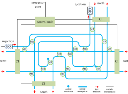 Optical routers are the key enabling components of optical NoCs. We proposed a high-performance low-power optical router, Cygnus, for optical NoCs. Cygnus is non-blocking and based on silicon microresonators. We compared Cygnus with other microresonator-based routers, and analyzed their power consumption, optical power insertion loss, and the number of microresonators used in detail. The results show that Cygnus has the lowest power consumption and losses, and requires the lowest number of microresonators. For example, Cygnus has 50% less power consumption, 51% less optical power insertion loss, and 20% less microresonators than the optimized traditional optical crossbar router. Comparing to a
 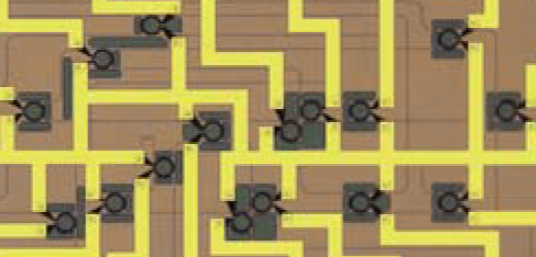 high-performance 45nm electronic router, Cygnus consumes 96% less power. Moreover, the passive routing feature of Cygnus guarantees that, while using dimension order routing algorithm, the maximum power consumption to route a packet through a network is a small constant number, regardless of the network size. For example, the maximum power consumption is 4.80fJ/bit under current technologies. We simulated and analyzed an 8x8 2D mesh NoC built from Cygnus and showed the end-to-end delay and network throughput under different offered loads and packet sizes.
Wave-Pipelined Interconnection
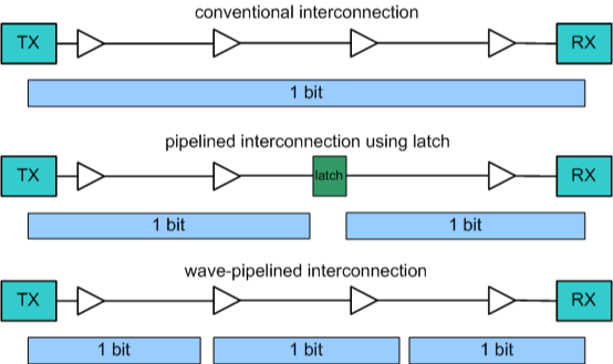 We proposed a new on-chip interconnection structure, wave-pipelined interconnection. Unlike traditional pipelining schemes, wave-pipelined interconnection is pipelined without using latches. Besides the wave-pipelining technique, the structure also uses misaligned buffers and interleaved lines to reduce crosstalk noise. Compared with current on-chip interconnections, wave-pipelined interconnection incurs less crosstalk, consumes less power, and achieves higher throughput. It can operate asynchronously and connect different clock domains. A 10 GHz clock rate is achieved on a 10 mm 8-bit bidirectional wave-pipelined interconnection in the 70 nm technology. SPICE simulations show that it reduces crosstalk by 88% and power consumption by 15% and increases throughput by 460% compared with current interconnections. Wave-pipelined interconnection provides on-chip communication architectures a more flexible and efficient building block.
General Design Methodology for On-Chip Communication Architectures
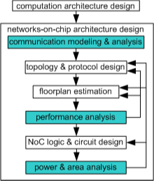 We proposed a general design methodology for on-chip communication architectures. Traditionally, each communication architecture has its own design methodology. This makes it difficult to compare and choose different communication architectures. Our methodology can explore the design space of on-chip communication more efficiently. It formalizes the on-chip communication architecture design, and makes it possible to design, model, and analyze all types of on-chip communication architectures in the same environment. Different communication architectures can be designed and compared based on the same standard. Our methodology has several features. First, it uses real communication traces to guide design and performance analysis. Second, it is based on circuit-level models and floorplans to estimate power and area. Third, it is compatible with current HW/SW codesign flows. Fourth, it makes use of widely available tools, such as OPNET, Design Compiler, and SPICE, which makes our methodology ready to use. Using the methodology, we designed the bus-based and crossbar-based architectures for a high-performance embedded video SoC in the 130 nm technology. Our analysis shows that the crossbar-based architecture achieves 62.5% higher performance with 82% less power consumption compared with the bus-based architecture. The crossbar-based architecture uses 88% less silicon area and 123% more metal area than the bus-based architecture. Our methodology also helps refine the crossbar-based architecture design and save additional 57% power.

